

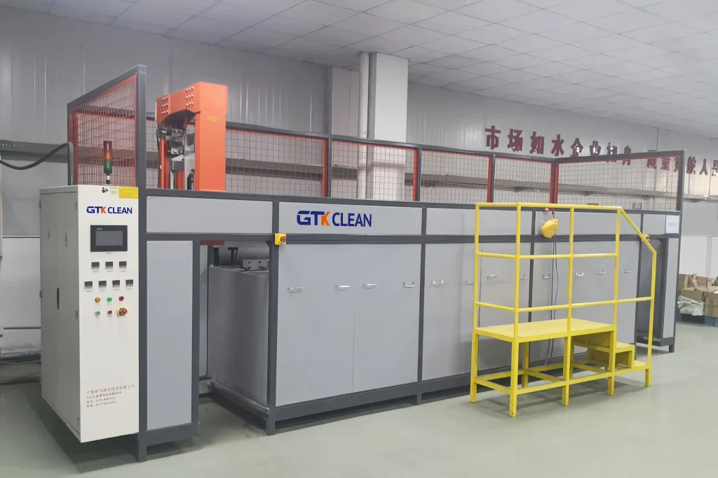
How to Clean Monocrystalline Silicon Wafers in the Semiconductor Industry?
As semiconductor materials technology continues to advance, higher standards are being set for wafer specifications and quality. Market demand for large diameter wafers ideal for microfabrication keeps growing steadily.
Today’s global manufacturers widely adopt advanced slicing, grinding, polishing and clean packaging processes, greatly upgrading wafer production technology. With the adoption of cutting-edge innovation, mass production has been realized for high-performance wafers such as SOI wafers.
To meet shrinking design rules, wafer manufacturers have ramped up equipment investment for 300 mm wafer production.
Ultrasonic cleaning technology delivers superior cleaning performance through frequency sweeping within a reasonable range. This motion creates gentle circulating flow in the cleaning solution, lifting contaminants from wafer surfaces and flushing them away quickly for higher cleaning efficiency.
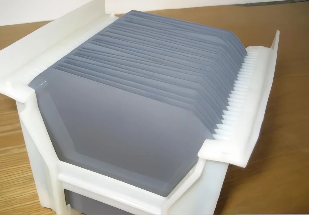
------Monocrystalline Silicon Wafer Reference Picture------
Cleaning Method & Placement
Place polished monocrystalline wafers horizontally on a slotted quartz rod frame above the bottom of the cleaning tank. Maintain a continuous flow of deionized water inside the tank, and run ultrasonic transducers mounted at the tank bottom at 40 kHz.
Flip each wafer every five minutes during the cycle until no dark residue appears on the wafer surface.
The cleaning tank is fitted with inlet and outlet ports on the side wall, with ultrasonic transducers installed underneath. A custom wafer holding frame sits inside the tank, featuring an open slotted quartz base positioned below the deionized water level. The entire frame is supported by mounting feet. In standard operation, the quartz rods are positioned 15 cm above the tank floor.
This horizontal layout replaces traditional vertical wafer cleaning. Vertical placement often traps contaminants on wafer surfaces and blocks ultrasonic energy transmission through soft wafer cassettes, resulting in uneven cleaning.Horizontal ultrasonic cleaning features a simpler structure, drastically reduces water consumption, and ensures full, consistent cleaning across the entire wafer surface.
Key Advantages of Ultrasonic Wafer Cleaning
- Vacuum degassing removes dissolved air from the solution. Combined with adjustable agitation motion, it strengthens soil removal, cuts down overall cleaning cycle time.
- Custom rotating basket design ensures even cleaning for integrated components and complex shaped parts that cannot be disassembled.
- Vacuum pressure extraction removes trapped air from blind holes, narrow gaps and stacked components, maximizing ultrasonic cleaning performance under reduced pressure.
- Integrated vapor cleaning and vacuum drying provide thorough surface treatment and long term surface protection.
- All vapor washing, drying and solution heating processes run under vacuum conditions, greatly improving operational safety.
- Explosion proof components and simplified heating systems further enhance site safety.
- Fully adjustable automatic temperature control for precise heating.
- Built in safety protection devices for stable, fail safe operation.
- Fine tunable ultrasonic output frequency to adapt to different cleaning requirements.
We appreciate your trust and support. We’re ready to communicate openly and partner with you on all your equipment needs.
You may contact us by email ([email protected]) or WhatsApp (+86 17768507147) for custom ultrasonic cleaning solutions.
Q&A
Q: What is a monocrystalline silicon wafer?
A: Silicon is a reactive non metallic element and a core crystalline material at the forefront of advanced new material development.Monocrystalline silicon features a complete, uniform lattice structure with directional physical properties and excellent semiconductor characteristics.Ultra high purity is required, reaching 99.9999%, and even exceeding 99.9999999% for premium semiconductor grades.
Q: Structure of monocrystalline silicon
A: When molten pure silicon solidifies, silicon atoms arrange in a diamond cubic lattice to form a continuous, ordered single crystal structure.Monocrystalline silicon exhibits metalloid properties with mild conductivity that rises with temperature, delivering stable intrinsic semiconductor performance at ultra high purity levels.
Q: Applications of monocrystalline silicon wafers
A: It serves as the core raw material for semiconductor silicon components, widely used in high power rectifiers, power transistors, diodes and switching electronic devices.
Q: Monocrystalline silicon production process
A: Raw material feeding → Melting → Necking growth → Shoulder expansion → Constant diameter growth → Tail growth.
Q: Alternative names for ultrasonic transducers
A: They are most commonly referred to as ultrasonic transducers or ultrasonic vibration elements.
Q: Installation requirements for ultrasonic transducers
A: Ultrasonic transducers can be mounted firmly on any flat, rigid metal surface in most industrial applications.
 English
  German
  Spanish
  French
  Russian
  Portuguese